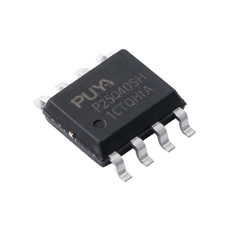
P25Q40SH-SSH-IT Serial Peripheral Interface SPI Non-volatile NOR Flash Memory Chip
1 Introduction
PUYA P25Q40SH Flash is a feature rich and cost-optimized serial peripheral interface (SPI) non-volatile NORflash family. This application note provides conversion guidelines for migrating from the P25Q40H to theP25Q40SH Flash.This application note is based on information available to date from datasheets and other application notespublicly available from PUYA. Please refer also to the latest relevant specifications. The document discussesthe specification differences when migrating from P25Q40H to P25Q40SH.
2 Feature Comparison and Differences
PUYA P25Q40H products are well suited for migration to PUYA P25Q40SH products. Some of the reasons arecompatible pinouts, packages, command set, and 4KB sector structure. Both P25Q40H and P25Q40SHdevices support Single (Standard) I/O, Dual I/O, and Quad I/O modes. The main differences betweenP25Q40H and P25Q40SH are listed in the table below:
Table 2-1. High Level Feature Support Comparison | Feature / Parameter | P25Q40H | P25Q40SH |
| Supple Voltage | 2.3V-3.6V | 2.3V-3.6V |
| Single (Standard) IO Operations | √ | √ |
| Dual IO Operations | √ | √ |
| Quad IO Operations | √ | √ |
| QPI | not support | √ |
| Standard Normal Read SCK Frequency (max) | 55 MHz | 55 MHz |
| Standard Fast Read SCK Frequency (max) | 104 MHz | 104 MHz |
| Dual Fast Read SCK Frequency (max) | 104 MHz | 104 MHz |
| Quad Fast Read SCK Frequency (max) | 104 MHz | 104 MHz |
| Software Protection | √ | √ |
| Individual Block Protection | not support | √ |
| One Time Programmable Region(s) | 3 x 512 Bytes | 3 x 512 Bytes |
| Buffer access | not support | √ |
| Erase(PE,SE,BE) time Typ. | 8ms | 16ms |
| Erase(CE) time Typ. | 8ms | 16ms |
| Configure Register | not support | √ |
| Temperature Range Option | -40C to +85C | -40C to +85C |
Table 2-1-1 Pin Descriptions | No. | Symbol | Extension | Remarks |
| 1 | CS# | Chip select | |
| 2 | SO SIO1 | Serial data output for 1 x I/O | Serial data input and output for 4 x I/O read mode |
| 3 | WP# SIO2 | Write protection active low | Serial data input and output for 4 x I/O read mode |
| 4 | GND | - | Ground of the device |
| 5 | SI SIO0 | Serial data input for 1x I/O | Serial data input and output for 4 x I/O read mode |
| 6 | SCLK | - | Serial interface clock input |
| 7 | HOLD#/RESET# SIO3 | Hardware Reset Pin Active low or to pause the device withoutdeselecting the device | Serial data input and output for 4 x I/O read mode |
| 8 | Vcc | - | Power supply of the device |


Packaging & Shipping
Standard export packaging available. Customers can choose from cartons, wooden cases, and wooden pallets according to their requirements.
Frequently Asked Questions
How to obtain the price?
We typically provide quotations within 24 hours of receiving your inquiry (excluding weekends and holidays). For urgent pricing requests, please contact us directly.
What is your delivery time?
Small batches typically ship within 7-15 days, while large batch orders may require approximately 30 days depending on order quantity and season.
What are your payment terms?
Factory pricing with 30% deposit and 70% balance payment via T/T before shipment.
Available shipping methods include sea freight, air freight, and express delivery (EMS, UPS, DHL, TNT, FEDEX). Please confirm your preferred method before ordering.